Internal Connection on FMLR Modules
Hardware application note on internal connection between MCU and transceiver on FMLR modules.
Abstract
All Miromico FMLR modules are a combination of an MCU and a transceiver chipset. This application note points out the details about the internal connection.
The internal connection includes:
- Interface between MCU and transceiver
- RF switch connection (power and control)
- Power supply of TXCO
FMLR-72-STM
Overview
| Net | MCU Pin | SX126x Pin | RF Switch Pin |
|---|---|---|---|
| Reset | PC2 | nReset | - |
| SPI MOSI | PB15 | MOSI | - |
| SPI MISO | PB14 | MISO | - |
| SPI SCK | PB10 | SCK | - |
| SPI CS | PA4 | NSS | - |
| DIO0 | PA1 | DIO0 | - |
| DIO1 | PA6 | DIO1 | - |
| DIO2 | PA7 | DIO2 | - |
| DIO3 | PC4 | DIO3 | - |
| DIO4 | PC5 | DIO4 | - |
| DIO5 | PB11 | DIO5 | - |
| VDD_SW | PB12 | - | VDD (power supply) |
| RXTX | - | RXTX | CTRL |
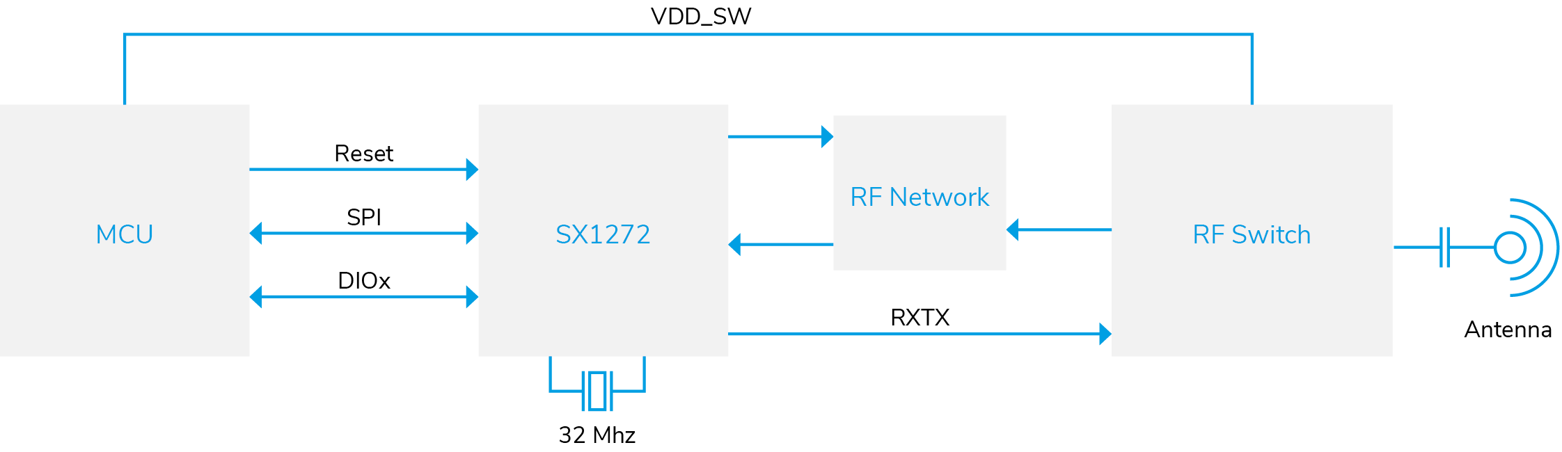
Transceiver
The SX1272 transceiver is connected to SPI2 and some additional GPIO pins of the STM32 MCU (see Overview).
Radio clock is generated by a crystal connected to the SX1272.
RF Path and Switch
The module integrates an RF switch to switch between RX and TX path. The RF switch is directly controlled by RXTX pin of the SX1272. To reduce power consumption, the RF switch can be powered down in case there is no active radio communication. The power supply (VDD) of the RF switch is connected to a GPIO pin of the MCU (see Overview).
Radio antenna output is AC coupled 50Ω output. Antenna matching needs to be done on the carrier board.
Info
There is no ESD protection on the radio module. If antenna pad is exposed, additional ESD protection is needed.
FMLR-61-STM
Overview
| Net | MCU Pin | SX126x Pin | RF Switch Pin |
|---|---|---|---|
| Reset | PB11 | nReset | - |
| SPI MOSI | PB15 | MOSI | - |
| SPI MISO | PB14 | MISO | - |
| SPI SCK | PB10 | SCK | - |
| SPI CS | PA4 | NSS | - |
| BUSY | PC4 | BUSY | - |
| DIO1 | PA1 | DIO1 | - |
| DIO2 | - | DIO2 | CTRL |
| DIO3 | - | DIO3 | - |
| VDD_SW | PB12 | - | VDD (power supply) |
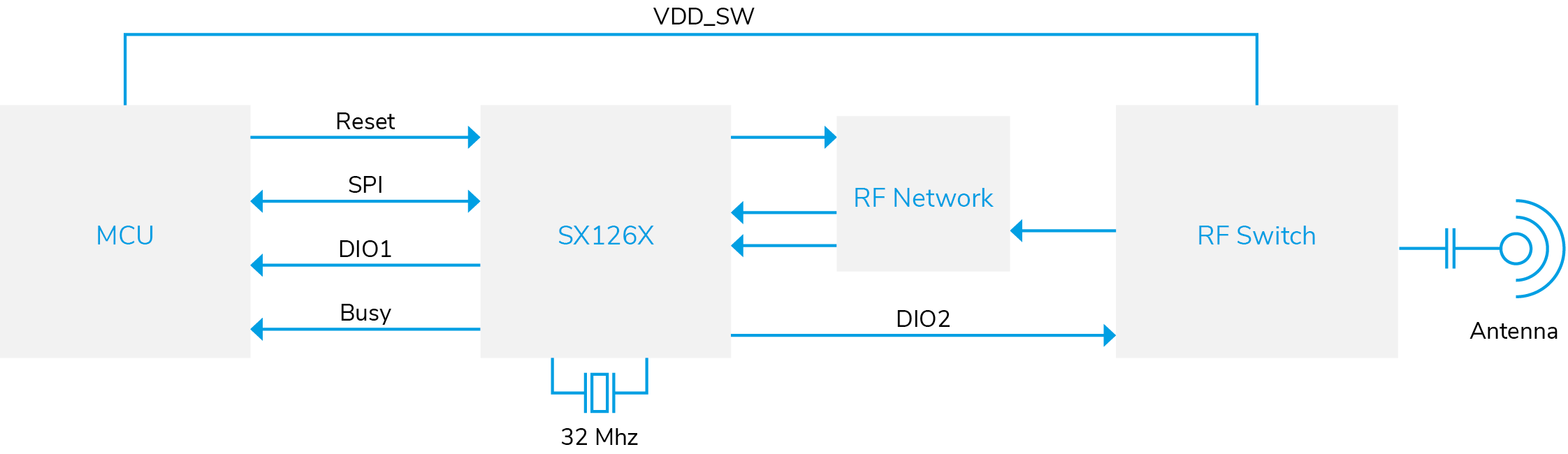
Transceiver
The SX126x transceiver is connected to SPI2 and some additional GPIO pins of the STM32 MCU (see Overview).
Radio clock is generated by a crystal connected to the SX126x. As the SX126x is providing internal load cap tuning for the crystal, the values have to be configured in the chipset accordingly. See SX126x product page for details and documentation.
RF Path and Switch
The module integrates an RF switch to switch between RX and TX path. The RF switch is directly controlled by DIO2 of the SX126x. To reduce power consumption, the RF switch can be powered down in case there is no active radio communication. The power supply (VDD) of the RF switch is connected to a GPIO pin of the MCU (see Overview).
Radio antenna output is AC coupled 50Ω output. Antenna matching needs to be done on the carrier board.
Info
There is no ESD protection on the radio module. If antenna pad is exposed, additional ESD protection is needed.
FMLR-80-STM
Overview
| Net | MCU Pin | SX126x Pin | TXCO |
|---|---|---|---|
| Reset | PC5 | nReset | - |
| SPI MOSI | PB15 | MOSI | - |
| SPI MISO | PB14 | MISO | - |
| SPI SCK | PB10 | SCK | - |
| SPI CS | PB12 | NSS | - |
| BUSY | PA1 | BUSY | - |
| DIO1 | PA6 | DIO1 | - |
| DIO2 | PA7 | DIO2 | - |
| DIO3 | PC4 | DIO3 | - |
| VDD_TXCO | PA4 | - | VDD (power supply) |
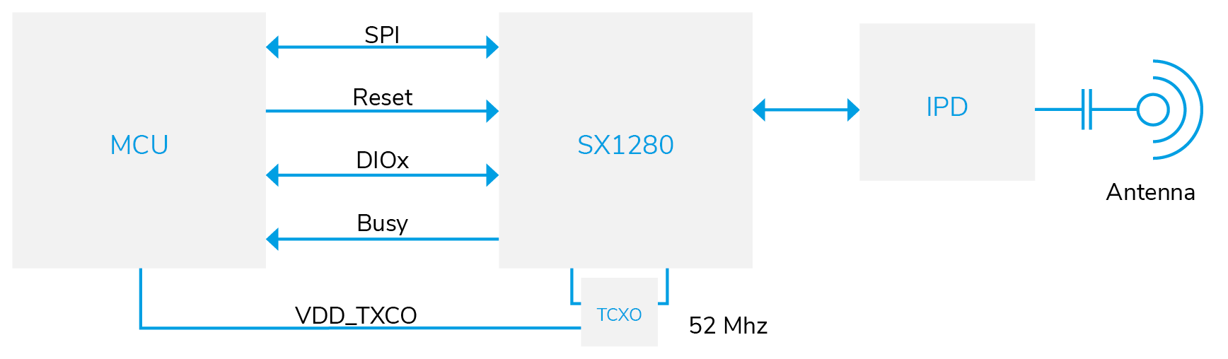
Transceiver
The SX128x transceiver is connected to SPI2 and some additional GPIO pins of the STM32 MCU (see Overview).
Radio clock is generated by a TCXO connected to the SX128x. Power to the TCXO is provided through MCU GPIO pin (see Overview). Consider TCXO startup times when switching power of the TCXO.
RF Path
Radio antenna output is AC coupled 50Ω output. Antenna matching needs to be done on the carrier board.
Info
There is no ESD protection on the radio module. If the antenna pad is exposed, additional ESD protection is needed.
FMLR-1110-STM
Overview
| Net | MCU Pin | SX126x Pin | TXCO |
|---|---|---|---|
| Reset | PC5 | nReset | - |
| SPI MOSI | PB15 | MOSI | - |
| SPI MISO | PB14 | MISO | - |
| SPI SCK | PB10 | SCK | - |
| SPI CS | PB12 | NSS | - |
| BUSY | PA1 | BUSY | - |
| DIO1 | PA6 | DIO1 | - |
| DIO2 | PA7 | DIO2 | - |
| DIO3 | PC4 | DIO3 | - |
| VDD_TXCO | PA4 | - | VDD (power supply) |
Transceiver
The SX128x transceiver is connected to SPI2 and some additional GPIO pins of the STM32 MCU (see Overview).
Radio clock is generated by a TCXO connected to the SX128x. Power to the TCXO is provided through MCU GPIO pin (see Overview). Consider TCXO startup times when switching power of the TCXO.
RF Path
Radio antenna output is AC coupled 50Ω output. Antenna matching needs to be done on the carrier board.
Info
There is no ESD protection on the radio module. If the antenna pad is exposed, additional ESD protection is needed.
FMLR-WL-STM
Overview
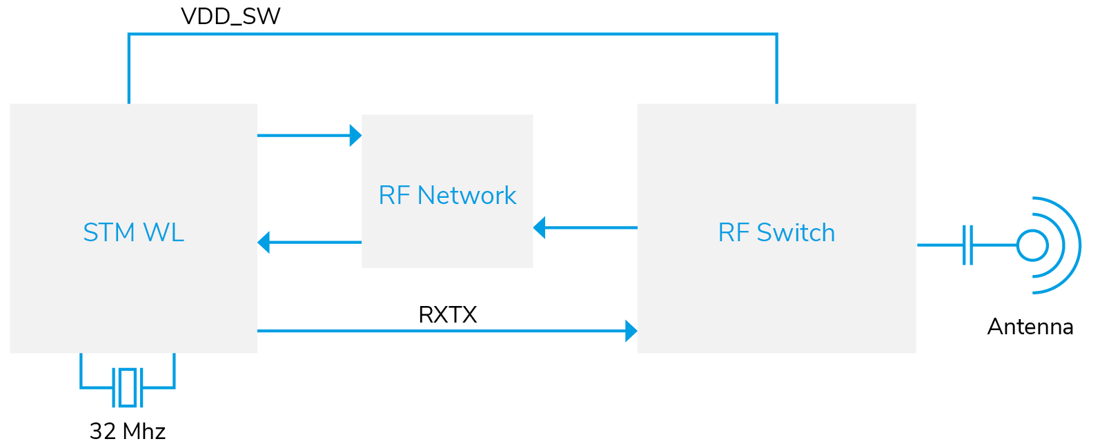
| Net | SoC Pin | RF Switch Pin |
|---|---|---|
| RXTX | PC3 | CTRL |
| VDD_SW | PC5 | VDD (power supply) |
RF Path
On the module, only the high-power (HP) transmission path is connected. The module integrates an RF switch to switch between RX and TX path. The RF switch is controlled by a GPIO.
To reduce power consumption, the RF switch can be powered down in case there is no active radio communication. The power supply (VDD) of the RF switch is connected to a GPIO pin of the MCU (see Overview).
Radio antenna output is AC coupled 50Ω output. Antenna matching needs to be done on the carrier board.
Info
There is no ESD protection on the radio module. If the antenna pad is exposed, additional ESD protection is needed.
FMLR-61-REN
Overview
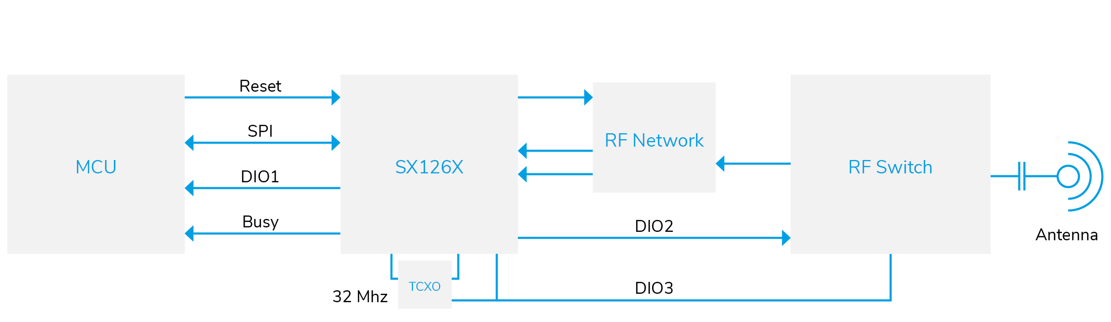
| Net | MCU Pin | SX126x Pin | RF Switch Pin | TCXO |
|---|---|---|---|---|
| Reset | P500 | nReset | - | - |
| SPI MOSI | P101 | MOSI | - | - |
| SPI MISO | P100 | MISO | - | - |
| SPI SCK | P102 | SCK | - | - |
| SPI CS | P103 | NSS | - | - |
| BUSY | P200 | BUSY | - | - |
| DIO1 | P015 | DIO1 | - | - |
| DIO2 | - | DIO2 | CTRL | - |
| DIO3 | - | DIO3 | VDD (power supply) | VDD |
Transceiver
The SX126x transceiver is connected to SPI and some additional GPIO pins of the Renesas S3A MCU (see Overview).
Radio clock is generated by a TCXO connected to the SX126x. Power to the TCXO is provided through DIO3 of the SX1261 See SX126x product page for details and additional documentation.
RF Path and Switch
The module integrates an RF switch to switch between RX and TX path. The RF switch is directly controlled by DIO2 of the SX126x. The power supply pin of the RF switch is connected to DIO3 of the SX126x to reduce power consumption in case there is no active radio communication.
Radio antenna output is AC coupled 50Ω output. Antenna matching needs to be done on the carrier board.
Info
There is no ESD protection on the radio module. If the antenna pad is exposed, additional ESD protection is needed.
FMLR-61-MAX
Overview
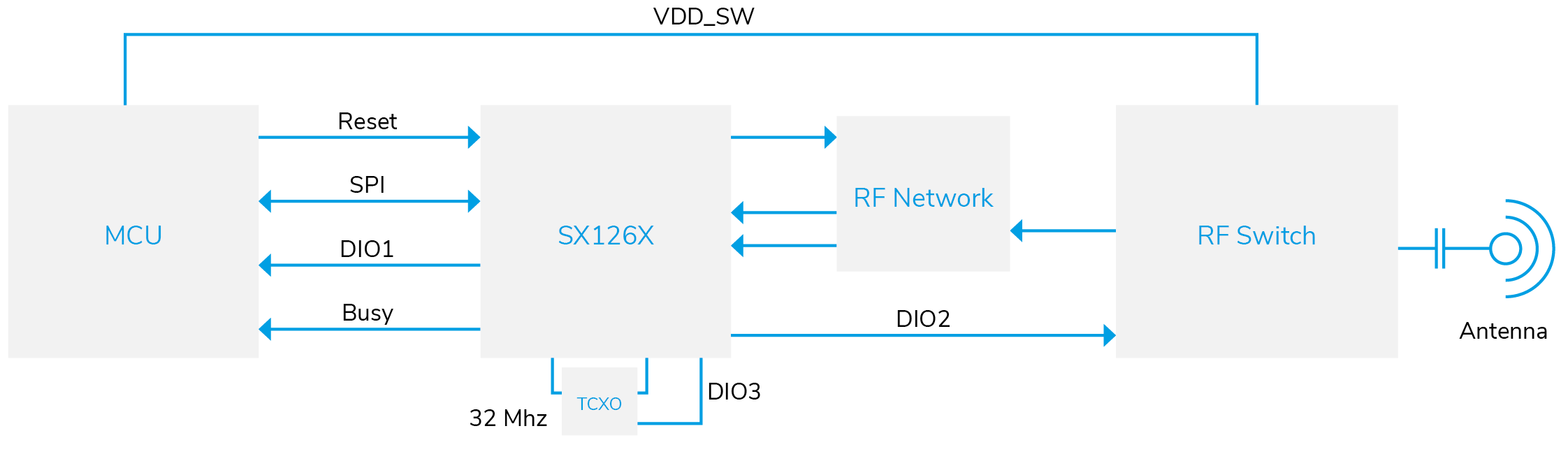
| Net | MCU Pin | SX126x Pin | RF Switch Pin | TCXO |
|---|---|---|---|---|
| Reset | P0.3 | nReset | - | - |
| SPI MOSI | P0.5 | MOSI | - | - |
| SPI MISO | P0.6 | MISO | - | - |
| SPI SCK | P0.4 | SCK | - | - |
| SPI CS | P0.7 | NSS | - | - |
| BUSY | P4.7 | BUSY | - | - |
| DIO1 | P4.6 | DIO1 | - | - |
| DIO2 | - | DIO2 | CTRL | - |
| DIO3 | - | DIO3 | VDD (power supply) | VDD |
| VDD_SW | P4.5 | - | VDD (power supply) | - |
Transceiver
The SX126x transceiver is connected to SPI and some additional GPIO pins of the MAX32625 MCU (see Overview).
Radio clock is generated by a TCXO connected to the SX126x. Power to the TCXO is provided through DIO3 of the SX1261 See SX126x product page for details and additional documentation.
RF Path and Switch
The module integrates an RF switch to switch between RX and TX path. The RF switch is directly controlled by DIO2 of the SX126x. To reduce power consumption, the RF switch can be powered down in case there is no active radio communication. The power supply (VDD) of the RF switch is connected to a GPIO pin of the MCU (see Overview).
Radio antenna output is AC coupled 50Ω output. Antenna matching needs to be done on the carrier board.
Info
There is no ESD protection on the radio module. If the antenna pad is exposed, additional ESD protection is needed.